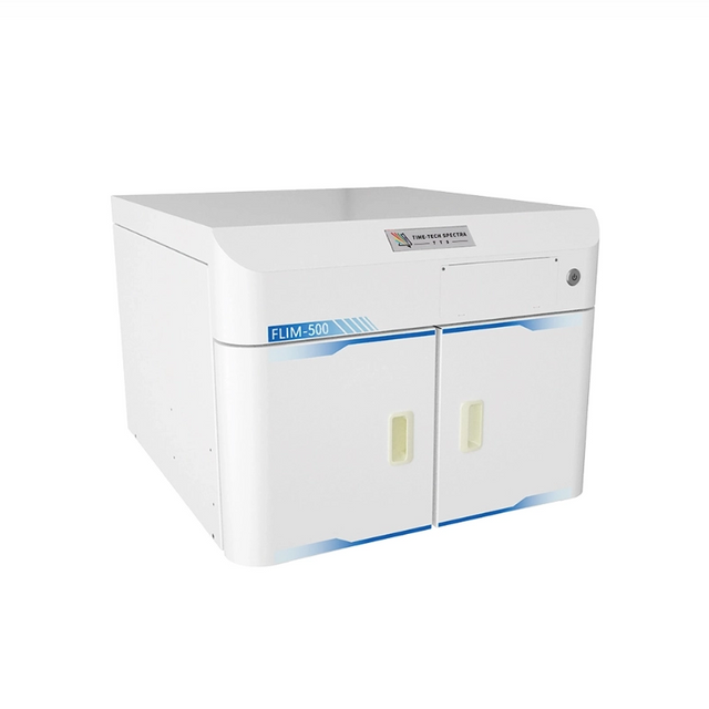
FLIM500Confocal Fluorescence Lifetime Imaging System
Connect spatial detail with fluorescence intensity, spectra and lifetime. FLIM500 combines a scanning microscope with configurable optical and electrical measurements for materials research.
Is FLIM500 right for your experiment?
For local imaging of emitting regions, lifetime variation and carrier dynamics in films, nanostructures and devices.
Manufacturer-listed values below distinguish the measurement parameter from its configuration conditions. The final quotation defines the supplied system.
FLIM500 specification guide
Parameter
Published value / capability
Configuration condition
Scanner band
400-900 nm
Galvanometer scanning system; not the full detector wavelength coverage.
Maximum image sampling
4096 × 4096 pixels
Pixel count does not specify optical resolution or field of view.
Objectives
10×, 50×, 100× air; optional 100× oil
Confirm working distance, numerical aperture and sample compatibility.
Spatial resolution
≤260 nm
Manufacturer specification with the 100× oil objective.
Spectrometer
300 mm monochromator
Select PMT or CCD detection.
Spectroscopy detector bands
PMT: 185-900 nm; CCD: 200-1100 nm
Detector ranges; usable system range also depends on the optics.
TCSPC detector bands
PMT: 200-870 nm; APD: 400-1100 nm
Select according to emission band and signal level.
TCSPC timing
≤70 ps time resolution listed on current supplier webpage
Module timing is not a guaranteed complete-system IRF.
TCSPC window
5 μs; 4096 bins
Long-lifetime expansion available.
Excitation choices
Discrete picosecond sources from 375 to 1060 nm
Select compatible wavelengths; optional supercontinuum source is not included by default.
Confirm microscope geometry for the quoted configuration: the 2026 catalogue describes an upright platform, while the supplier webpage describes an inverted platform. The sources also use different TCSPC timing descriptions. Confirm the full excitation-detector IRF rather than equating timing electronics with measured lifetime resolution.
410-2400 nm source listed as an option; this does not extend every microscope or detector path to that range.
Sample environment
The manufacturer demonstrates low-temperature and high-pressure imaging configurations.
Sample environment configuration
Compatibility
Check chamber geometry, objective working distance, thermal conditions and optical access.
Electrical & carrier imaging
Add device-contact and acquisition arrangements for electrical or carrier-dynamics studies.
Electrical & carrier imaging configuration
Device inputs
Provide contact drawings, bias/pulse conditions and whether EL, photocurrent or fixed-excitation carrier imaging is required.
Measurement examples
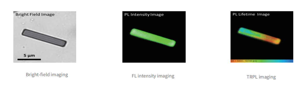
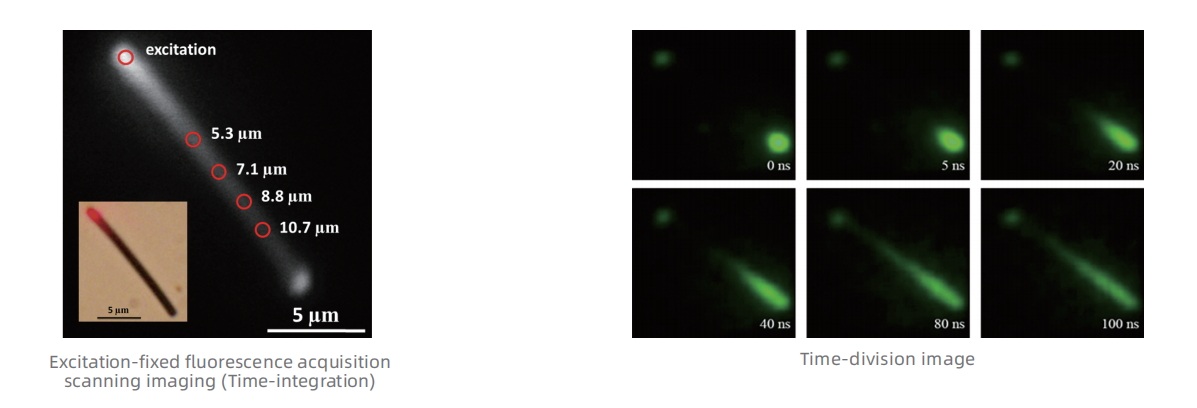
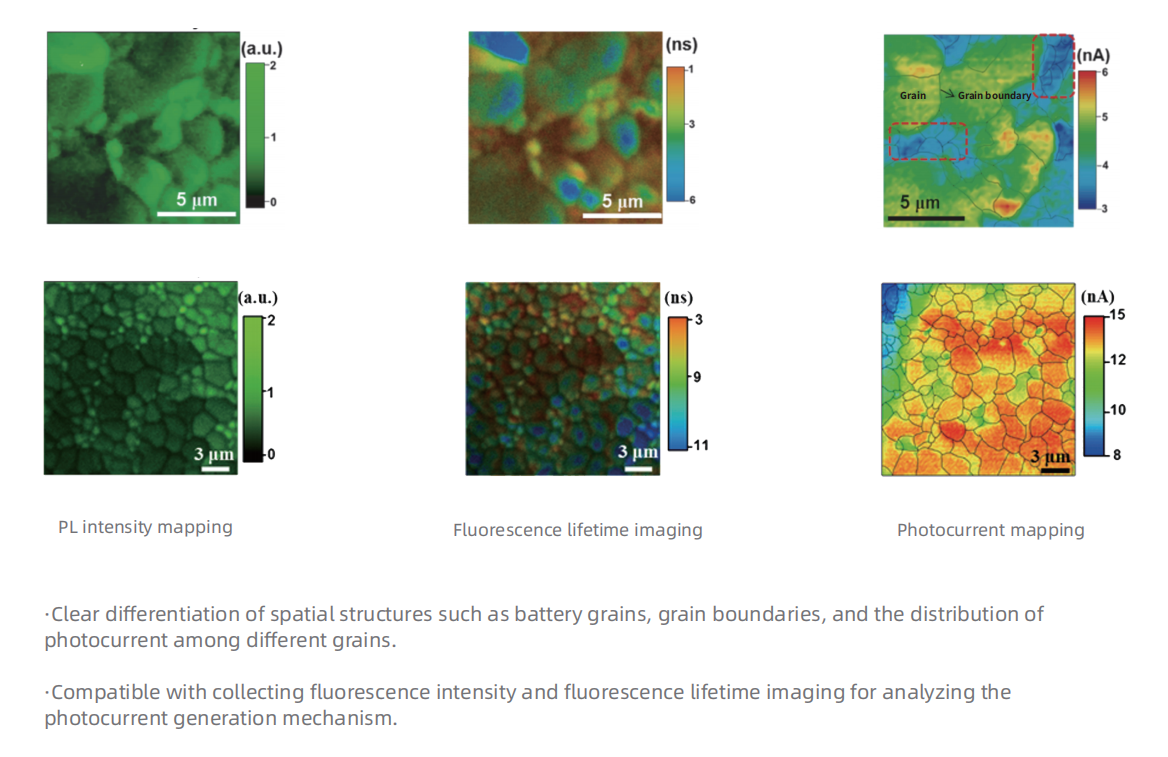
Original Time-Tech Spectra figures, not HX measurements. Axes, scales and plotted data are retained. Example performance depends on the sample and acquisition conditions.
MAPbI₃ nanowires · intensity and lifetime
Compare a bright-field view with emission intensity and lifetime information. A bright region alone does not establish a longer lifetime or improved material quality.
Fixed-excitation nanowire fluorescence and time-division images
Perovskite device · photocurrent mapping
Spatial photocurrent information complements optical emission measurements. Electrical contacting and the relevant measurement interface must be included in the configuration.
Send substrate thickness, sample size and which side is accessible to the objective. Confirm upright or inverted geometry with HX Technology.
Signal & imaging
Provide emission band, expected lifetime, field of view and required spatial detail; state any photobleaching limits.
Environment & installation
Confirm chamber or contact access, vibration isolation, instrument footprint, power and laser-safety needs for the complete configuration.
Selection questions
Does a 4096 × 4096 image guarantee 260 nm resolution?
No. Image sampling, field of view and optical resolution are different. The stated spatial resolution requires the specified oil objective and suitable measurement conditions.
When should I compare Solarium-L?
When the main question concerns photovoltaic material or device performance, including PLQE, QFLS or pseudo-J-V mapping. FLIM500 emphasises local fluorescence and lifetime imaging.